What The Tech?! Printed Circuit Boards

As we’ve explored the development of consumer electronics, you may have noticed a few themes starting to shine through as we’ve examined different components and looked at their effect on manufacturing.
There’s miniaturization, for portability and usability. We’ve got efficient batteries for on-the-go usage, and deep discharge to give us a longer life. And increased manufacturing ability, allowing for the production of thousands of devices in a short period.
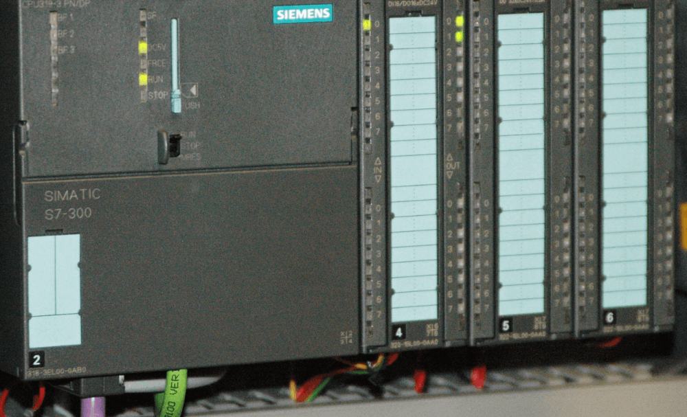
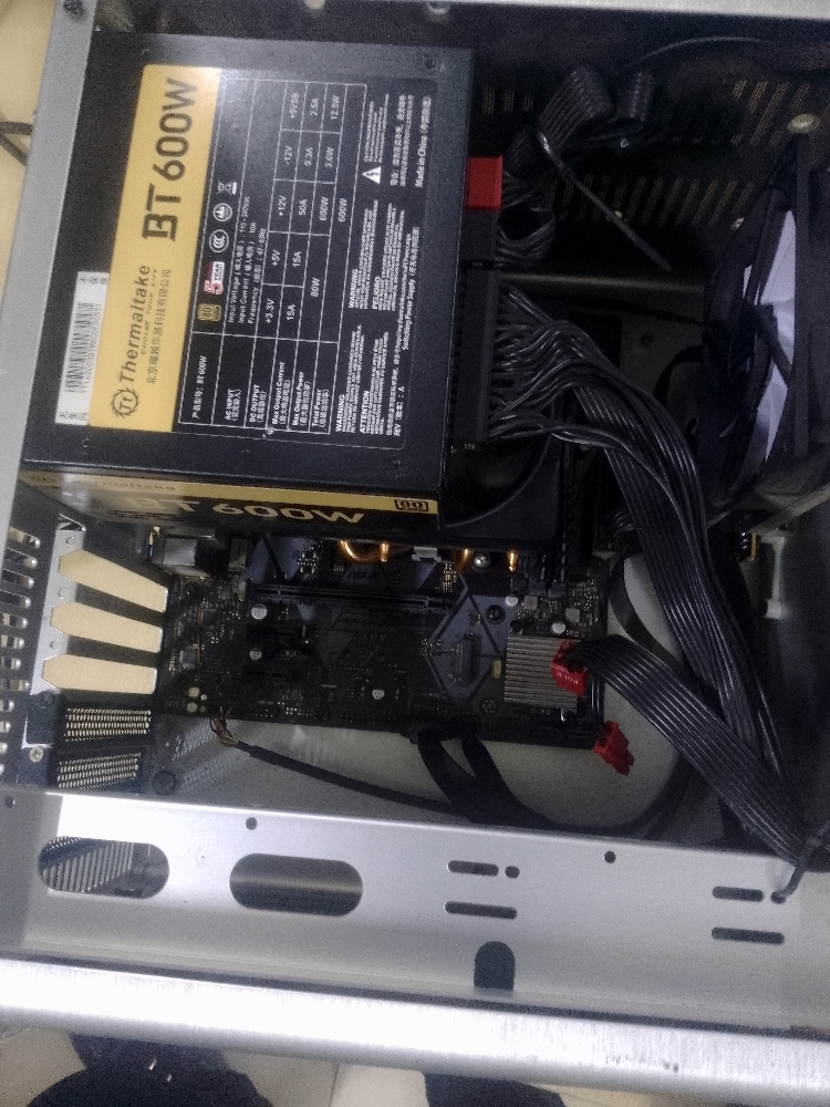
In today’s What The Tech, we’ll be exploring a component that makes all this happen. It’s in almost every electronic device that you can think of and made mass production faster and more attainable. Today, we’ll be looking at the history of the humble printed circuit board (PCB).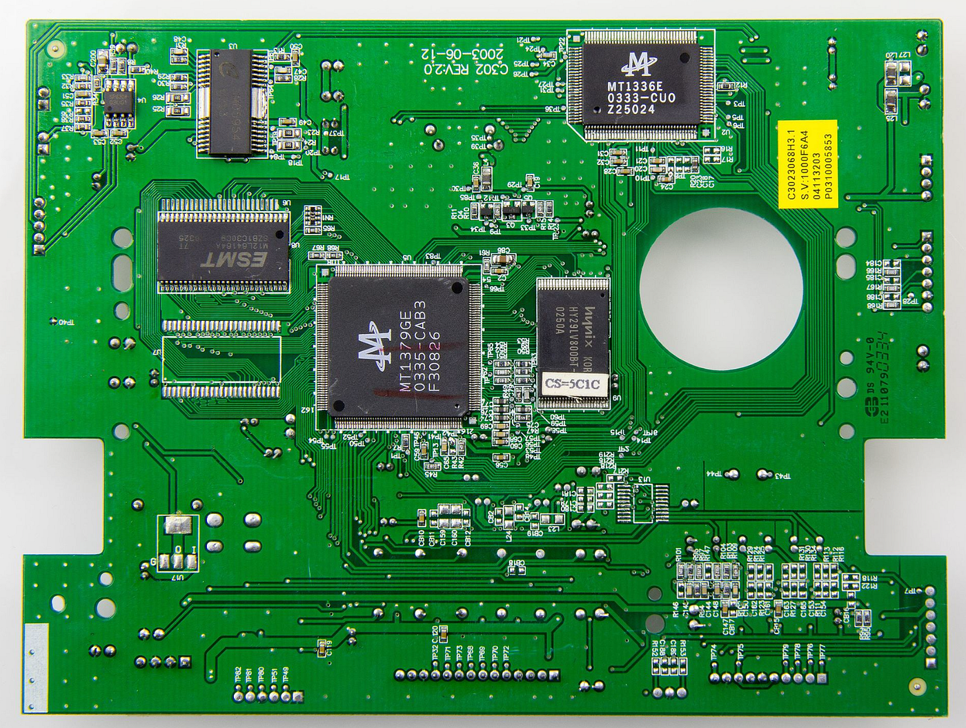 The mass production of consumer goods was easier with printed circuit boards. Source: Wikipedia
What Is It
Brought to life in the manufacturing chaos that was World War 2, the printed circuit board offered a new standard for manufacturing electronics. Before this, electronics used custom, hand-made boards that were custom-made for each project.
While the PCB used the same concept, it was more efficient due to its manufactured design and ability to have components spaced closely together. It also introduced the “batch” process whereby thousands of identical boards were produced to provide mass assembly on the production line. As components became smaller and more intricate, this process allowed for the rapid and cheap production of the consumer electronics we’ve come to know and love (and sometimes hate). The first proximity sensors had a military application, like these artillery shell fuses produced in WW2. Source: Wikipedia
The first patent for the PCB would come nearly two decades earlier though. In 1925, Charles Ducas filed the first patent for screen-printed electronics boards, and shortly after this experiments and refinement commenced.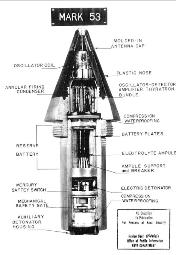 The Mk53 artillery shell used new, proximity fusing technology. Source: Wikipedia.
Like many other research programs, a war economy was kind to the printed circuit board. Despite being a relatively new technology at the time, a large amount of research was poured into the device.
As such, reliability improved and production costs dropped. The biggest wartime usage of the PCB was used in the production of VT fuse artillery shells. With an entirely misleading name, VT shells inferred that the firing mechanism was timing-based. However, the reality was, that the PCB allowed for fast production of the new proximity fuse, which used proximity-sensing technology to fire.
The proximity fuse is still used in air-to-air missiles, artillery shells, and other military applications to this day. The AIM-120 AMRAAM uses proximity sensor tech, bringing technology to air combat. Source: Wikipedia.
Commecialisation & Refinement
As the war came to a close and production shifted from military equipment to consumer goods, the PCB took on a new importance. It was due to this investment in consumer technology that would allow the PCB to face literally decades of development and refinement. This would include the shift to integrated circuits and smaller, surface mount components. As a result, many goods would end up becoming far smaller in size, and more power-efficient to boot.
The first of the most relevant improvements came with photoengraved boards, allowing for smaller and more precise manufacturing techniques to be established. After this, we saw the introduction of double-sided boards into the 60s as well as a new focus on environmental concerns, with lead-free boards becoming commonplace into the 1990s.
As the smartphone took hold and chips became smaller, we saw a greater focus on size and efficiency as well.
With all these refinements in play, the circuit board led to some major revolutions in consumer electronics. The craziest thing is, that most of these improvements occurred behind the scenes, with the average consumer showing little awareness of the generational differences that occurred across different devices. By the 90s, consumer tech had reached stratospheric levels. Source: Wikipedia
All we knew was that devices were becoming cheaper, smaller, and more power efficient, leading to a significant increase in the end-user experience along with a decreased technical penalty for entry. This meant consumers could do more while knowing less. A productivity dream!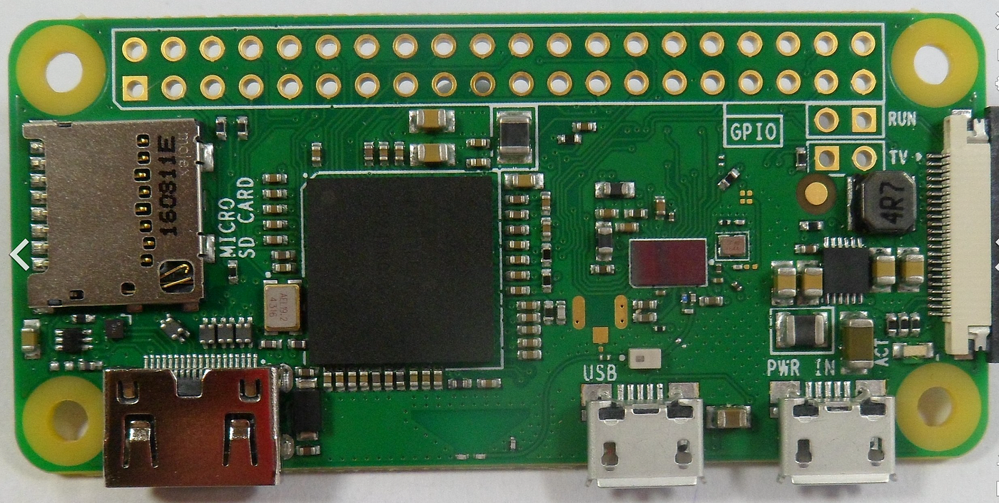 Miniaturization led to improved technology, like the Raspberry Pi Zero. Source: Wikipedia.
New and Improved Technology
With the explosion of smartphones and Internet Of Things-enabled devices, you’d be forgiven for thinking that the development of the Printed Circuit Board has peaked out, with little to return in the way of manufacturing efficiency or power dividends. And while you’d be right in saying new technology has provided new benefits, the fact is that the development of PCBs is still really mid-stride as opposed to being at the end of the road.
We see the AI revolution giving us AI-designed and implemented boards, leading to more efficient designs. Flexible / Wearable devices will benefit from being able to use a flexible PCB rather than a rigid piece of early 2000’s design. And the explosion of 3d printing into…..well everything really, means that we should continue to see 3d printed boards used as a way to provide cost efficiency on small or custom runs of electronics.
New improvements in materials science also allow us to make these boards more efficiently and cheaply. While this has manufacturing peaks, it’s reasonable to assume that as research continues around this process, devices will become more energy efficient while increasing their overall computing power at the same time.
These new materials also provide a potential solution to one of the biggest issues faced by consumer electronics as well, the safe disposal and processing of these systems once they reach the end of life. While traditionally the compounds used to manufacture these products come with a significant environmental penalty, the use of biodegradable boards and components offers a new opportunity to reduce the environmental footprint that comes with leveraging electronic systems.
In Closing
These pieces are written to bring light to subjects that don’t always see the light of day. However, despite this many of the innovations, we’ve discussed lead to a dramatic improvement in life expectancy as well as the overall quality of life. The circuit board is probably the most relevant of these, as despite being in literally everything we use, many people couldn’t even tell you what PCB stands for!
While we don’t need to know the physics behind every process nor why some things are done the way they are, one thing we do need to know is that understanding some of these processes a little better does actually come with some benefits. For instance, the humble little PCB as well as chips in general are highly relevant to things like geopolitics, something that affects our modern world nearly every single day.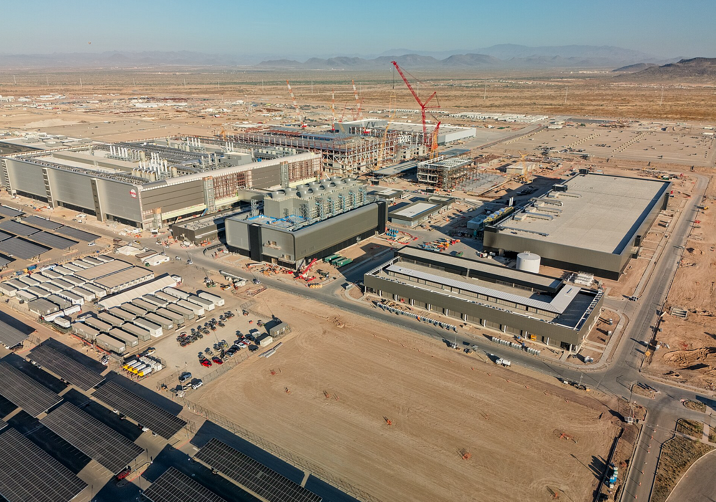 This US-based, production plant shows the global impact of Chips & PCB’s on world affairs. It’s essential for the modern world to function. Source: Wikipedia
As consumers, understanding the process lets us understand the importance of the goods. We can also argue for the right to repair and advocate for more environmentally safe components and products. While we won’t have to produce our own manufacturing line, we can advocate for some of these safer practices from those who do build these products.
Any net benefit we can encourage around this process would have major ramifications on manufacturing worldwide. A net positive, you could say.
Medium has recently made some algorithm changes to improve the discoverability of articles like this one. These changes are designed to ensure that high-quality content reaches a wider audience, and your engagement plays a crucial role in making that happen.
If you found this article insightful, informative, or entertaining, we kindly encourage you to show your support. Clapping for this article not only lets the author know that their work is appreciated but also helps boost its visibility to others who might benefit from it.
🌟 Enjoyed this article? Support our work and join the community! 🌟
💙 Support me on Ko-fi: Investigator515
📢 Join our OSINT Telegram channel for exclusive updates or
📢 Follow our crypto Telegram for the latest giveaways
🐦 Follow us on Twitter and
🟦 We’re now on Bluesky!
🔗 Articles we think you’ll like:
- Software Defined Radio & Radio Hacking
- OSINT Unleashed: 5 Essential Tools for Cyber Investigators
✉️ Want more content like this? Sign up for email updates here