Nano-size computer chip

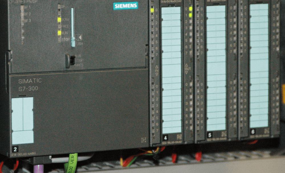
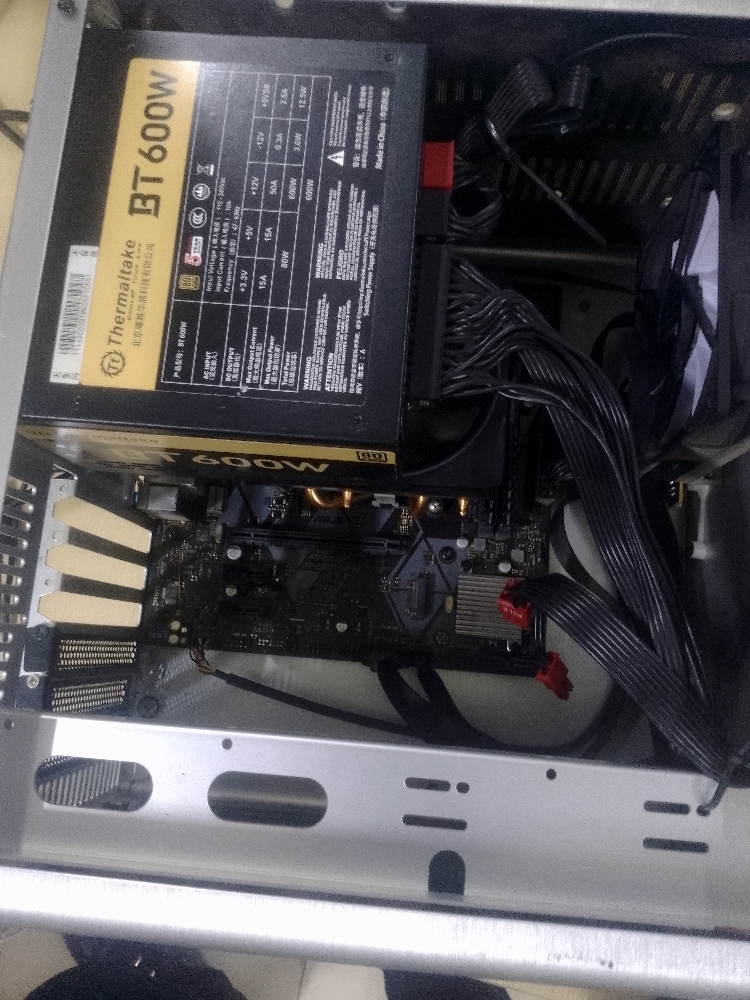
Basics of Computer chip manufacturing
Our mobile phones/computers are getting more powerful and smaller every year, these devices have more and faster functions on new models. This is because the computer chip manufacturers are able to pack more electronic circuits in the integrated circuit chip with semiconductor wires smaller than 10 Nano-meters (the size of one human hair is 100,000 Nano-meter), that’s incredibly small for humans to handle because 1 Nano meter can only fit 2 atoms. In the manufacturing process. The very tiny electronic wires are basically etched into the sizes and patterns by laser beam technology (extreme ultra-violet light beams named eUV). We should call it Nano-chip instead of Micro-chip as microns are bigger sizes than Nano.
It is called semiconductors because the materials-silicons/metal/other chemcials compound made it behaves like half a conductor half an insulator so to achieve binary status of 0-1 for computer functions.
Currently in the world, only TSMC-Taiwanese company and Samsung-South Korean company are the two East Asian companies that make the finest computer chips in the world (with 7 Nano-meters in conductor wires size), at this size humans probably approached saturation. Japanese lost the race as they use different technology and went down the wrong path with a dead end. S Korea is in a very close race with Taiwan but TSMC slightly ahead. However the materials that are used for the manufacturing come from Japan and S Korea. The Europeans Ducth and Germans produce the machines/parts to do the manufacturing job.
Burn Lin-Taiwan Chinese was first to propose immersion Lithography in 1980s, he had been working for TSMC from 2000 and helping the Ducth company named ASML and TSMC to develop the eUV resolution method to approach atomic size for etching of Nano-size electronic circuits patterns. In simple terms, this technology enable the laser beam to refract in the water immersion and produce better resolution and finer focus onto the semiconductor wafers that approach nano-size. 

You can see the water immersion refract the laser beam more than the dry air method and therefore improve the resolution for finer etching of the semiconductor wires to smaller size.
Conclusion :
Humans probably achieved saturation in Nano-chip innovations because any conductor size smaller than 7 nano meters would not able to hold the atoms together with the structure to conduct electric currents fluently. So we are likely forced to use different technology like quantum mechanics to make more powerful computers or quantum computers, the technology can basically facilitate electric current to go forward and backward at the same time as quantum mechanics theory stated that an electron can exist in two locations at the same time at sub-atomic level. That's called quantum weirdness which is another topic.
Sources :
https://en.wikipedia.org/wiki/Burn-Jeng_Lin
https://en.wikipedia.org/wiki/Extreme_ultraviolet_lithography